JAPAN DISPLAY
(주)리젠웍스는 JDI Korea Distributer로 자동차부터 웨어러블까지 모든 산업문야에 TFT LCD와 관련 솔루션을 공급하는 디스플레이 전문 회사입니다.
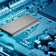
TOSHIBA MCU & SEMICONDUCTOR
(주)리젠웍스는 Toshiba Korea Distributer로 Micom Solution 개발 및 전자부품을 판매하는 반도체 전문 회사 입니다.
GET STARTED NOWKIOXIA
(주)리젠웍스는 KIOXIA Korea Distributer로 플래시 메모리 및 SSD 분야의 기술적 리더십과 광범위한 제품 포트폴리오를 통해 고객의 요구를 해결합니다.
FORTIOR TECHNOLOGY
(주)리젠웍스는 Fortior Distributer로 모터 토탈 제어 솔루션을 제공하는 전문 기업입니다. 산업용, 가전제품, 자동차 등 다양한 분야에서 혁신적인 모터 제어 기술을 통해 효율성과 신뢰성을 향상시키고 있습니다.
GREAT POWER
(주)리젠웍스는 GREAT POWER Distributer로 배터리 및 에너지 저장 솔루션을 전문으로 하는 글로벌 선도 기업입니다. 리튬 이온 배터리, 니켈 수소 배터리, 에너지 저장 시스템 등 다양한 제품을 통해 전기차, 에너지 저장, 스마트 디바이스 등 여러 산업에 혁신적인 에너지 솔루션을 제공합니다.

반도체 솔루션
고객의 니즈에 맞춘 반도체 솔루션을 제공하여 다양한 산업에 기여하고 있습니다.
디스플레이 솔루션
첨단 디스플레이 기술을 활용하여 최상의 품질과 서비스를 제공합니다.

맞춤형 고객 지원
다양한 고객의 요구에 맞춘 맞춤형 기술 지원과 최상의 고객 서비스를 제공합니다.
우리는 Regenworks입니다
Regenworks는 고객에게 반도체 및 디스플레이 솔루션을 제공하는 전문 기업으로, 고객의 성공을 위한 최고의 기술력과 서비스를 제공합니다.
우리는 혁신적인 기술 개발과 고객 맞춤형 솔루션을 통해 반도체 및 디스플레이 시장에서의 입지를 확고히 하고 있습니다. 다양한 산업에 기여하며 미래를 위한 솔루션을 제공합니다.